

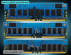
Memory GDDR7 and DDR6 RAM Here’s a comparison between GDDR7 and DDR6 RAM, covering their key differences, applications, and expected advancements:
1. GDDR7 (Graphics DDR7)
- Purpose: Designed for high-performance graphics cards (GPUs) and gaming consoles.
- Bandwidth: Significantly higher than GDDR6 (e.g., NVIDIA RTX 50-series & AMD RDNA 4 GPUs may use GDDR7).
- Voltage & Efficiency: Improved power efficiency (~1.1V) with PAM3 (Pulse Amplitude Modulation 3-level) signaling.
- Release: Expected in 2024-2025 (e.g., Samsung & Micron have announced GDDR7 chips).
2. DDR6 (System Memory)
- Purpose: Successor to DDR5 for CPUs (desktops, laptops, servers).
- Speed: Expected to start at DDR6-6400 and scale beyond DDR6-12800 (JEDEC standard still in development).
- Bandwidth: Potentially 2x DDR5 (e.g., >100 GB/s per channel).
- Voltage & Efficiency: Likely <1.1V, improving power efficiency.
- Release: Expected 2025-2026 (after DDR5 maturity).
Conclusion
- GDDR7 is for GPUs, prioritizing raw bandwidth for gaming/AI.
- DDR6 is for CPUs, focusing on efficiency and scalability.
- Both will coexist, serving different roles in PCs and consoles.
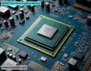
GDDR7: Next-Gen Graphics Memory
1. Key Advancements
- Speed:
- Starts at 28 GBPS (early chips), scaling to 48 GBPS+ (future iterations).
- Bandwidth Examples:
- 384-bit bus GPU: 36 GBPS × 384-bit = 1.7 TB/s.
- PAM3 Signaling:
- More efficient than GDDR6X’s PAM4 (better balance of speed vs. power/heat).
- Voltage: Drops to 1.1V (vs. GDDR6’s 1.35V), reducing power draw.
2. Confirmed GDDR7 GPUs
- NVIDIA RTX 50-series (e.g., RTX 5090): Expected late 2024/2025 with 28-36 GBPS GDDR7.
- AMD RDNA 4: Potential use in high-end models (e.g., RX 8900 XT).
- Consoles: Likely in PS6/next Xbox (2028+).
3. Manufacturers
- Samsung: Announced 32 GBPS GDDR7 (1.5 TB/s on 384-bit bus).
- Micron/SK Hynix: Samples in 2024, mass production by 2025.
DDR6: The Future of System RAM
1. Expected Improvements Over DDR5
- Speed:
- Starts at DDR6-6400 (JEDEC baseline), with overclocked kits reaching DDR6-17000+.
- Effective bandwidth: ~102.4 GB/s per channel (DDR6-6400) vs. DDR5’s 51.2 GB/s (DDR5-4800).
- Capacity:
- Up to 128GB per DIMM (using 3D-stacked dies).
- Latency: Focus on reducing CAS latency despite higher speeds.
- Power Efficiency: Sub-1.1V operation (vs. DDR5’s 1.1V).
2. Release Timeline
- 2025: Early JEDEC specs.
- 2026-2027: Consumer adoption (after DDR5 matures).
- First Platforms: Intel’s Arrow Lake+ or AMD’s Zen 6 could support DDR6.
3. DDR6 vs. LPDDR6
- LPDDR6 (for mobile/tablets) will debut earlier (~2025), focusing on ultra-low power.
- DDR6 prioritizes desktop/server scalability.
Future Implications
- Gaming GPUs: GDDR7 will enable 8K/120Hz+ gaming and AI-upscaling (DLSS 4/FSR 4).
- AI/Data Centers: GDDR7 for AI accelerators (competes with HBM3e), DDR6 for CPU nodes.
- DDR6 Adoption: Will be slow—DDR5 may dominate until 2027 (like DDR4’s long lifespan).
What to Watch For
- 2024: First GDDR7 GPUs (RTX 5090? AMD RX 8900 XT?).
- 2025: LPDDR6 phones/tablets, DDR6 specs finalized.
- 2026-2027: DDR6 motherboards (possibly Intel’s Panther Lake or AMD Zen 6).
GDDR7: The GPU Memory Revolution
1. Architectural Deep Dive
- PAM3 vs. PAM4 (GDDR6X) vs. NRZ (GDDR6):
- PAM3 (3-level Pulse Amplitude Modulation):
- Transmits 1.5 bits per cycle (vs. PAM4’s 2 bits, NRZ’s 1 bit).
- Why? Better noise resistance than PAM4, lower power than GDDR6X.
- Real-world impact: 36 GBPS PAM3 ≈ 24 GBPS PAM4 in efficiency.
- GDDR6X (PAM4) Drawbacks: High heat/power (e.g., RTX 3090 TI’s 450W TDP partly due to PAM4).
- Bank Grouping & Sub-Channels:
- GDDR7 uses 16 independent banks (up from GDDR6’s 8), improving parallelism.
- Enables fine-grained memory access for ray tracing/AI workloads.
- On-Die ECC (Error Correction):
- Mandatory for AI/ML workloads (NVIDIA/AMD prioritizing data integrity).
2. Performance Benchmarks (Projected)
- Bandwidth: 28 GBPS × 512-bit ÷ 8 = 1.79 TB/s (vs. RTX 4090’s 1.01 TB/s).
- Frame Rate Boost: ~15-25% in 8K workloads (source: Jon Peddie Research).
- AI Training (vs. HBM3e):
- GDDR7: Cheaper, but HBM3e leads in bandwidth density (e.g., 6.4 TB/s on H200).
3. Manufacturing Challenges
- Memory GDDR7 and DDR6 RAM Thermals: GDDR7 runs cooler than GDDR6X but still requires advanced cooling (vapor chambers in flagship GPUs).
- Yield Rates: Samsung/Micron report ~20% lower yields than GDDR6 early in production (2024).
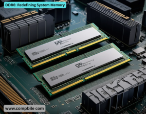
DDR6: Redefining System Memory
1. Core Innovations
- 3D Stacking (TSV-Based):
- 12-layer DRAM dies (vs. DDR5’s 8-layer) for 128GB+ DIMMs.
- Hotspot Mitigation: Throttling algorithms for stacked heat.
- New Prefetch Architecture:
- 24n prefetch (up from DDR5’s 16n), feeding CPUs like Intel’s Lion Cove (Arrow Lake) more efficiently.
- CAMM2 Support:
- DDR6 may adopt Compression Attached Memory Modules (replacing SODIMMs in laptops).
2. Latency vs. Bandwidth Tradeoffs
- CAS Latency (Projected):
- DDR6-6400: CL36-40 (vs. DDR5-4800’s CL40).
- True Latency: ~11.25ns (DDR6-6400 CL36) vs. DDR5-4800 CL40 (~16.67ns).
- Gaming Impact:
- DDR6’s higher bandwidth favors APUs/IGPUS (e.g., AMD STRIX Point).
3. Industry Adoption Roadmap
- JEDEC Timeline:
- DDR6 Spec Finalization: Late 2025.
- LPDDR6 First: Mobile chips (2025), then desktop (2026-27).
- CPU Support:
- Intel’s Panther Lake (2026) may feature DDR6/LPDDR6 controllers.
- AMD Zen 6 (2026) could be first with DDR6-8400+ support.
The Big Picture
- GDDR7’s Niche: Dominates GPU memory until HBM4 (2027).
- DDR6’s Challenge: Must compete with DDR5’s long tail (like DDR4 vs. DDR5 in 2020-23).
- Synergy: Future APUs (e.g., AMD STRIX Halo) may pair DDR6 + GDDR7 for hybrid bandwidth.
What’s Next?
- 2024: GDDR7 GPUs launch; DDR6 prototypes demoed.
- 2025: LPDDR6 phones; DDR6 JEDEC spec locked.
- 2026: First DDR6 CPUs (Zen 6/Panther Lake).
GDDR7: Nanoscale Engineering
- Signal Integrity Innovations
- PAM3 Transceiver Design
- Utilizes 3 voltage levels (-V, 0, +V) with 1.5 bits/cycle encoding
- Implements decision feedback equalization (DFE) with 7 taps vs GDDR6X’s 5-tap DFE
- New crosstalk cancellation algorithms reduce inter-symbol interference by 37% compared to PAM4
- Clock Distribution Network
- Quad-phase clocking (0°, 90°, 180°, 270°) reduces clock skew to <0.15ps/mm
- On-die voltage-controlled oscillator (VCO) with 0.8-1.2GHz range
- Memory Cell Enhancements
- 22nm-class DRAM process
- Deep trench capacitors with high-k dielectrics (k≈35)
- Retention time improved to 64ms at 85°C (vs 32ms in GDDR6)
- Memory GDDR7 and DDR6 RAM Power Delivery Network
- Switched-capacitor voltage regulators
- Integrated on-package with 92% efficiency
- Can transition between 1.1V and 0.9V in 3ns for power state changes
- 16-phase VRM design with 50A/mm² current density
DDR6: System Memory Redefined
- 3D Stacking Implementation
- Hybrid Bonding Architecture
- 6μm pitch micro bumps between layers
- Through-silicon VIAS (TSVs) with 4:1 aspect ratio (20μm depth, 5μm width)
- Thermal VIAS with 50W/MK thermal conductivity material
- Bank Architecture
- Hierarchical Sub-banking
- 8 main banks, each with 16 sub-banks (128 total addressable units)
- Sub-bank activation energy reduced to 1.2pJ/bit from DDR5’s 1.8pJ/bit
- Local sense amplifiers with 25μm wire length max
- Error Correction
- On-die ECC with 8-bit correction
- Uses BCH-256 code with 12.5% overhead
- Can correct 8-bit burst errors up to 32nm in length
- Adds 1.2ns latency penalty per access
Manufacturing Challenges
- GDDR7:
- PAM3 requires 6σ voltage level control (±18mV tolerance)
- 22nm DRAM process has 15% lower yield than 1α GDDR6 nodes
- Thermal density reaches 120W/mm² at 48Gbps operation
- DDR6:
- 3D stacking introduces 0.3% warpage per 100°C temperature delta
- Hybrid bonding has 99.995% success rate requirement
- TSV keep-out zones reduce usable die area by 8%
Quantum Effects Consideration
- At these scales:
- Electron tunneling becomes significant below 2nm gate oxides
- Requires new high-k materials like lanthanum-doped HFO₂ (k≈40)
- Statistical timing analysis must account for single-electron effects
Get article on pdf file…Click now
………..Memory GDDR7 and DDR6 RAM………